- 您现在的位置:买卖IC网 > Sheet目录2006 > LTC2754AIUKG-16#PBF (Linear Technology)IC DAC 16BIT QUAD IOUT 52-QFN
LTC2754
20
2754f
APPLICATIONS INFORMATION
Op Amp Selection
Because of the extremely high accuracy of the 16-bit
LTC2754-16, careful thought should be given to op amp
selection in order to achieve the exceptional performance
of which the part is capable. Fortunately, the sensitivity of
INL and DNL to op amp offset has been greatly reduced
compared to previous generations of multiplying DACs.
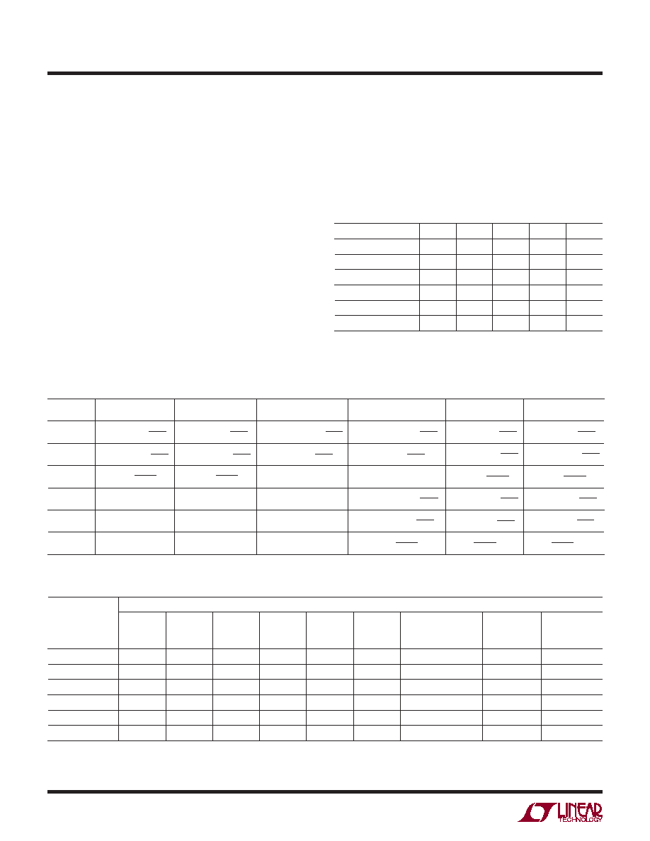
Tables 4 and 5 contain equations for evaluating the effects
of op amp parameters on the LTC2754’s accuracy when
programmed in a unipolar or bipolar output range. These
are the changes the op amp can cause to the INL, DNL,
unipolar offset, unipolar gain error, bipolar zero and bipolar
gain error. Tables 4 and 5 can also be used to determine
the effects of op amp parameters on the LTC2754-12.
However, the results obtained from Tables 4 and 5 are
in 16-bit LSBs. Divide these results by 16 to obtain the
correct LSB sizing.
Table 6 contains a partial list of LTC precision op amps
recommended for use with the LTC2754. The easy-to-use
design equations simplify the selection of op amps to meet
Table 4. Coefcients for the Equations in Table 5
OUTPUT RANGE
A1
A2
A3
A4
A5
5V
1.1
2
1
10V
2.2
3
0.5
1.5
±5V
2
1
1.5
±10V
4
0.83
1
2.5
±2.5V
1
1.4
1
–2.5V to 7.5V
1.9
3
0.7
0.5
1.5
A3 VOS1 19.8
IB1 0.13
0
A4 VOS2 13.1
A4 IB2 0.13
A4
()
5V
VREF
()
5V
VREF
()
16.5k
AVOL1
OP AMP
VOS1 (mV)
IB1 (nA)
AVOL1 (V/V)
VOS2 (mV)
IB2 (mV)
AVOL2 (V/V)
VOS1 3.2
IB1 0.0003
A1
0
INL (LSB)
()
5V
VREF
()
5V
VREF
()
1.5k
AVOL1
()
66k
AVOL2
()
131k
AVOL1
()
131k
AVOL1
()
131k
AVOL2
()
131k
AVOL2
VOS1 0.82
IB1 0.00008
A2
0
DNL (LSB)
()
5V
VREF
()
5V
VREF
A3 VOS1 13.2
IB1 0.13
0
UNIPOLAR
OFFSET (LSB)
()
5V
VREF
()
5V
VREF
()
5V
VREF
VOS1 13.2
IB1 0.0018
A5
VOS2 26.2
IB2 0.26
BIPOLAR GAIN
ERROR (LSB)
()
5V
VREF
()
5V
VREF
()
5V
VREF
()
5V
VREF
BIPOLAR ZERO
ERROR (LSB)
UNIPOLAR GAIN
ERROR (LSB)
()
5V
VREF
()
5V
VREF
()
5V
VREF
()
5V
VREF
()
5V
VREF
VOS1 13.2
IB1 0.0018
A5
VOS2 26.2
IB2 0.26
Table 5. Easy-to-Use Equations Determine Op Amp Effects on DAC Accuracy in All Output Ranges (Circuit of Page 1). Subscript 1
Refers to Output Amp, Subscript 2 Refers to Reference Inverting Amp.
Table 6. Partial List of LTC Precision Ampliers Recommended for Use with the LTC2754 with Relevant Specications
AMPLIFIER
AMPLIFIER SPECIFICATIONS
VOS
μV
IB
nA
AVOL
V/mV
VOLTAGE
NOISE
nV/√Hz
CURRENT
NOISE
pA/√Hz
SLEW
RATE
V/μs
GAIN BANDWIDTH
PRODUCT
MHz
tSETTLING
with LTC2755
μs
POWER
DISSIPATION
mW
LT1001
25
2
800
10
0.12
0.25
0.8
120
46
LT1097
50
0.35
1000
14
0.008
0.2
0.7
120
11
LT1112 (Dual)
60
0.25
1500
14
0.008
0.16
0.75
115
10.5/Op Amp
LT1124 (Dual)
70
20
4000
2.7
0.3
4.5
12.5
19
69/Op Amp
LT1468
75
10
5000
5
0.6
22
90
2
117
LT1469 (Dual)
125
10
2000
5
0.6
22
90
2
123/Op Amp
发布紧急采购,3分钟左右您将得到回复。
相关PDF资料
LTC2755AIUP-16#PBF
IC DAC 16BIT CUR OUT 64-QFN
LTC2757ACLX#PBF
IC DAC 18BIT PAR 48LQFP
LTC2758AILX#PBF
IC DAC 18BIT SPI/SRL 48-LQFP
LTC2844IG#TRPBF
IC TXRX 3.3V MULTIPROTCOL 28SSOP
LTC2852MPS#PBF
IC TXRX RS485 20MBPS 14-SOIC
LTC486ISW#TRPBF
IC DVR RS485 LOW PWR QUAD 16SOIC
LTC490IS8#TRPBF
IC TXRX RS485 LOW POWER 8-SOIC
LTC491IS#TRPBF
IC TXRX RS485 LOW POWER 14-SOIC
相关代理商/技术参数
LTC2754AIUKG-16#TRPBF
功能描述:IC DAC 16BIT QUAD IOUT 52-QFN RoHS:是 类别:集成电路 (IC) >> 数据采集 - 数模转换器 系列:SoftSpan™ 产品培训模块:Data Converter Fundamentals
DAC Architectures 标准包装:750 系列:- 设置时间:7µs 位数:16 数据接口:并联 转换器数目:1 电压电源:双 ± 功率耗散(最大):100mW 工作温度:0°C ~ 70°C 安装类型:表面贴装 封装/外壳:28-LCC(J 形引线) 供应商设备封装:28-PLCC(11.51x11.51) 包装:带卷 (TR) 输出数目和类型:1 电压,单极;1 电压,双极 采样率(每秒):143k
LTC2754BCUKG-16#PBF
功能描述:IC DAC 16BIT QUAD IOUT 52-QFN RoHS:是 类别:集成电路 (IC) >> 数据采集 - 数模转换器 系列:SoftSpan™ 标准包装:1 系列:- 设置时间:4.5µs 位数:12 数据接口:串行,SPI? 转换器数目:1 电压电源:单电源 功率耗散(最大):- 工作温度:-40°C ~ 125°C 安装类型:表面贴装 封装/外壳:8-SOIC(0.154",3.90mm 宽) 供应商设备封装:8-SOICN 包装:剪切带 (CT) 输出数目和类型:1 电压,单极;1 电压,双极 采样率(每秒):* 其它名称:MCP4921T-E/SNCTMCP4921T-E/SNRCTMCP4921T-E/SNRCT-ND
LTC2754BCUKG-16#TRPBF
功能描述:IC DAC 16BIT QUAD IOUT 52-QFN RoHS:是 类别:集成电路 (IC) >> 数据采集 - 数模转换器 系列:SoftSpan™ 产品培训模块:Data Converter Fundamentals
DAC Architectures 标准包装:750 系列:- 设置时间:7µs 位数:16 数据接口:并联 转换器数目:1 电压电源:双 ± 功率耗散(最大):100mW 工作温度:0°C ~ 70°C 安装类型:表面贴装 封装/外壳:28-LCC(J 形引线) 供应商设备封装:28-PLCC(11.51x11.51) 包装:带卷 (TR) 输出数目和类型:1 电压,单极;1 电压,双极 采样率(每秒):143k
LTC2754BIUKG-16#PBF
功能描述:IC DAC 16BIT QUAD IOUT 52-QFN RoHS:是 类别:集成电路 (IC) >> 数据采集 - 数模转换器 系列:SoftSpan™ 产品培训模块:Data Converter Fundamentals
DAC Architectures 标准包装:750 系列:- 设置时间:7µs 位数:16 数据接口:并联 转换器数目:1 电压电源:双 ± 功率耗散(最大):100mW 工作温度:0°C ~ 70°C 安装类型:表面贴装 封装/外壳:28-LCC(J 形引线) 供应商设备封装:28-PLCC(11.51x11.51) 包装:带卷 (TR) 输出数目和类型:1 电压,单极;1 电压,双极 采样率(每秒):143k
LTC2754BIUKG-16#TRPBF
功能描述:IC DAC 16BIT QUAD IOUT 52-QFN RoHS:是 类别:集成电路 (IC) >> 数据采集 - 数模转换器 系列:SoftSpan™ 产品培训模块:Data Converter Fundamentals
DAC Architectures 标准包装:750 系列:- 设置时间:7µs 位数:16 数据接口:并联 转换器数目:1 电压电源:双 ± 功率耗散(最大):100mW 工作温度:0°C ~ 70°C 安装类型:表面贴装 封装/外壳:28-LCC(J 形引线) 供应商设备封装:28-PLCC(11.51x11.51) 包装:带卷 (TR) 输出数目和类型:1 电压,单极;1 电压,双极 采样率(每秒):143k
LTC2754CUKG-12#PBF
功能描述:IC DAC 12BIT QUAD IOUT 52-QFN RoHS:是 类别:集成电路 (IC) >> 数据采集 - 数模转换器 系列:SoftSpan™ 产品培训模块:Data Converter Fundamentals
DAC Architectures 标准包装:750 系列:- 设置时间:7µs 位数:16 数据接口:并联 转换器数目:1 电压电源:双 ± 功率耗散(最大):100mW 工作温度:0°C ~ 70°C 安装类型:表面贴装 封装/外壳:28-LCC(J 形引线) 供应商设备封装:28-PLCC(11.51x11.51) 包装:带卷 (TR) 输出数目和类型:1 电压,单极;1 电压,双极 采样率(每秒):143k
LTC2754CUKG-12#TRPBF
功能描述:IC DAC 12BIT QUAD IOUT 52-QFN RoHS:是 类别:集成电路 (IC) >> 数据采集 - 数模转换器 系列:SoftSpan™ 标准包装:47 系列:- 设置时间:2µs 位数:14 数据接口:并联 转换器数目:1 电压电源:单电源 功率耗散(最大):55µW 工作温度:-40°C ~ 85°C 安装类型:表面贴装 封装/外壳:28-SSOP(0.209",5.30mm 宽) 供应商设备封装:28-SSOP 包装:管件 输出数目和类型:1 电流,单极;1 电流,双极 采样率(每秒):*
LTC2754IUKG-12#PBF
功能描述:IC DAC 12BIT QUAD IOUT 52-QFN RoHS:是 类别:集成电路 (IC) >> 数据采集 - 数模转换器 系列:SoftSpan™ 产品培训模块:Data Converter Fundamentals
DAC Architectures 标准包装:750 系列:- 设置时间:7µs 位数:16 数据接口:并联 转换器数目:1 电压电源:双 ± 功率耗散(最大):100mW 工作温度:0°C ~ 70°C 安装类型:表面贴装 封装/外壳:28-LCC(J 形引线) 供应商设备封装:28-PLCC(11.51x11.51) 包装:带卷 (TR) 输出数目和类型:1 电压,单极;1 电压,双极 采样率(每秒):143k